Mosfet power amplifier
Products related to this product are for sale in the webshop. The mosfet amplifier is available as a complete kit (PCB + components) or PCB-only, so you can buy the components yourself.

Introduction
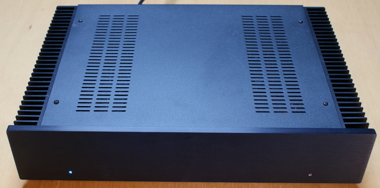
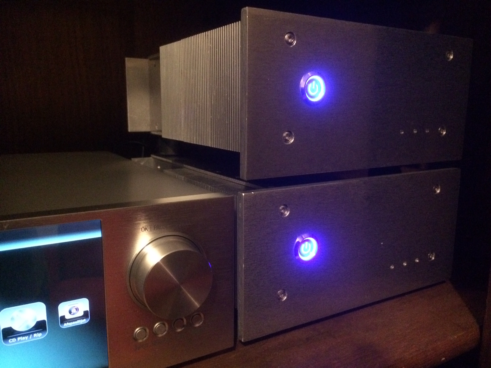
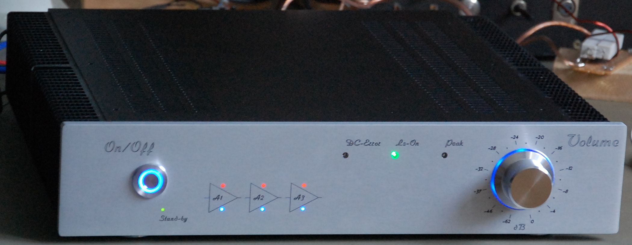
Some time ago, I ordered a book at Amazon named High Power Audio Amplifier Construction Manual by Randy Slone. This book is very much recommended for any one who wants to design an audio amplifier. After reading this book, I decided to try and design a mosfet power amplifier myself, you can read about the result below. I am very pleased with the result, which is really a high-end power amplifier. Not only it looks pretty cool, but also the measurements and listening tests show that this is a top class amplifier, for which I believe there is little room for improvements.
Specifications
- Max output power: 100W@8ohm, 150W@4ohm
- THD+N (1kHz): < 0.003%
- Noise level: < -100 dB
- Input sensitivity: 1.2V rms
- Input impedance: 22kohm
- Bandwidth: 100kHz
- Voltage gain: 27dB
- Slew rate: 15V/us
- PCB dimensions: 100x60mm
Design
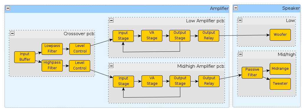
The main idea behind the design is to build a bi-amping amplifier with separate amplifier boards for the low and mid/high section of each channel, but of course you can also build a normal version by only using one amplifier pcb per channel. The line input signal goes to an active Linkwitz-Riley crossover (-24 dB/decade rolloff) with a crossover frequency at 330 Hz. Both outputs of the crossover pcb are amplified with identical amplifier pcb’s. Four of them are needed for a stereo amplifier. The output of the low frequency amplifier goes to the woofer of a 3-way speaker. The output of the mid/high frequency amplifier goes to the midrange/tweeter of the speaker.
Amplifier schematic
The amplifier is a quite conventional 3-stage design, with input stage, voltage amplifier stage and output stage, which uses a pair of Hitachi lateral MOSFET’s (2SJ162/2SK1058). Apart from the MOSFET’s only common and easily available components are used. Component values are not shown, but you can buy the PCB or a complete kit in the shop.
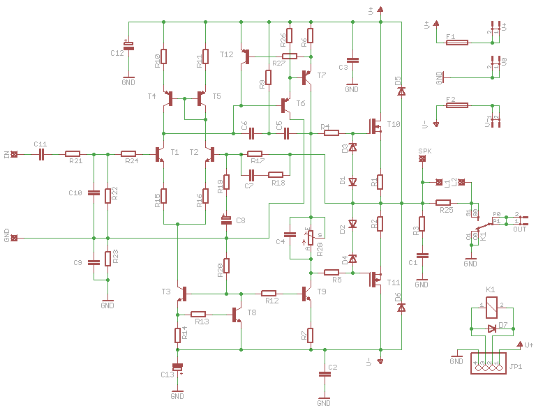
The input signal enters the amp through C11 to remove DC (crossover at 7Hz) and is then lowpass filtered (crossover at 130kHz) to prevent high frequency radio signals from entering. The input impedance of 22k is mainly determined by R22. Components around T3 form a current source that feeds the long tailed pair (T1+T2). A current mirror consisting of T4+T5 takes care of balancing the current trough the two legs of the LTP. Various emitter degeneration resistors are used to apply local feedback to the transistors and makes operation less sensitive to all kind of variations (temperature, transistor parameters, etc)
This amplifier uses two pole compensation (C5, C6, R9) and an extra driving transistor (T6) to achieve very low distortion levels in the VA stage. The VA stage itself uses a current source (components around T9) and the voltage on the gates of the MOSFETS is controlled by T7. Using R8 the quiescent current through the MOSFETS can be set to decrease crossover distortion. Short circuit protection has been incorporated in the VA stage (R27+T12), which limits the max current through the VA stage to some 20mA. This way, the protection will only have effect when the load connected is less than about 2 ohm (and a large input signal is present).
The Mosfets in the output stage are equipped with zener diodes for basic protection. The global feedback loop is closed by connecting the output through R17 and R19 to the base of T2. AC gain of the amplifier is only determined by the values of R17 and R19 (set to a common 27dB). DC gain is ‘1’ because of C8. The output is connected to the speakers through a damped inductor (L+R25) and output relay. Zobel network (C1+R3) and damped inductor give improved stability for difficult loads.
Supply considerations
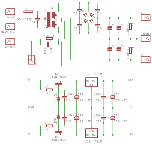
A schematic of the proposed supply for this amplifier is shown in the following picture. Mains voltage is connected to the primary winding of a preferably toroidal transformer with center-tapped secondary winding. Fuse F1 needs to be chosen in line with your transformer rating. Capacitor C1 prevents high frequency noise from entering/leaving the amp through the supply. Rectification is done with bridge rectifier B1 (or use 4 high power fast recovery diodes). Snubbing capacitors C2-C5 short high frequency switching of the diodes and result in a much cleaner supply. The output of the rectifier is filtered using reservoir capacitors C6-C9. Cheaper and better is to use more low-valued capcitors in parallel, as an example I use 12 times a 2200uF electrolytic capacitor giving 13.200uF per rail. Bleeder resistors R2 and R3 will make sure that the capacitors are safely discharged when you turn off the amplifier.
Always make sure the rail voltage to the amplifiers is taken directly from the capacitors, not from the rectifier. Make a star ground connection (HQGND) by using separate wires to all ground connections in the amplifier including the speaker connections, which is even more important when constructing a stereo amplifier. The mains Earth connection must be connected directly to the chassis of the amplifier. The connection from chassis to the star ground connection using R1 will prevent ground loops and C10 will short high frequency noise.
The bottom part of the figure is only needed if you also need a dual 15V opamp supply, e.g. for a LR filter or integrated preamp. The opamp supply is constructed from the rail voltage in 2 steps: first there is a stepdown converter, which reduces the input voltage for the voltage regulators. The stepdown converter for the positive side consists of R4, D2, C21, which gives a constant 20V at the base of Q2. At the emitter of Q2 this gives approximately 19.3V, which is a nice input voltage for the 7815. The capacitors around IC2 are quite standard, with C16 for instability prevention under varying loads. The negative side works in a similar but mirrored way. This circuit can deliver a maximum of about 150mA, where main power dissipation is done in IC1 and IC2. The power dissipation in IC2 equals (V+ - 19.3)*IQ2 so with a 48V supply and 150mA this is 4.3W, which can only be achieved with a proper heatsink.
To make the construction of the power supply easier, I designed 2 supply pcb’s: a supply pcb with room for 16 electrolytic capacitors of 18mm diameter and a supply pcb with integrated 15V dual supply with room for 12 electrolytic capacitors of 18mm diameter. The 2200uF/63V 105deg capacitors I use fit on this pcb giving 2x13.200 uF and 2x17.600 uF respectively. If you think that is not enough, you can even use two (or more) of them, but measurements below show that already excellent results are achieved with 2x13.200 uF!
To achieve 100W in an 8 ohm load, 28.3Vrms or 40V peak is needed at the output. Due to the fact that a MOSFET output stage is used, about 48V rail voltage is needed to achieve this. Taking into account a 1V voltage drop in the rectifier, the needed transformer voltage is (48+1)/1.41 = 34.75V, so a dual 35V transformer would be about perfect. Most manufacturers of toroidal transformers specify their voltage rating under load, so the unloaded rail voltage will be some volts higher.
The rms current needed for 100W in 8 ohm would be 28.3Vrms/8ohm=3.54A rms. Thus for a mono amplifier, the minimum transformer VA rating would become 35*3.54=124VA. To give some extra current margin, a 150VA transformer would be great. If you intend to drive a 4 ohm load, this needs to be doubled. If you construct a stereo amplifier, this obviously needs to be doubled (again).
Output relay configuration
The output relay is used to disconnect the speakers from the output of the amp and can be switched directly from the positive supply. A test with a 48V relay showed that it switches already at 27V, which allows a large supply range. The output relay can be used in different modes:
- Immediately from the pcb, by connecting V+ and GND from the board to the relay using two jumpers on the pinheader (connect 1+2 and 3+4). You might hear a thump when amp is switched on however.
- Using external protection circuitry, you can use the SPK pin for monitoring the output stage voltage.
An external protection circuit is strongly recommended and can be used for some or all of these functions:
- Delayed switch on
- Loss of AC detection
- DC protection
- Amplifier instability protection
A complete microcontroller based protection circuit with the above functions is now available, more information on the PicProtection project page.
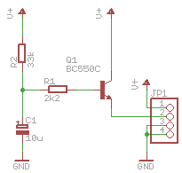
Below is a very simple circuit to prevent the thumb when the amplifier is switched on. It gives only a delayed switch on, so no DC protection. You can easily build it on vero board and connect it to the pinheader on the amp board. For convenience this RelayDelay circuit is now also available as pcb or kit. Its working principle is very simple: when the amp is switched on, C1 is being charged through R2, therefore the voltage on the base of Q1 is slowly increasing and with it the voltage on the emitter of Q1, until the relay switches. With the current values of R2 and C1, it takes about 4s before the relay switches, bit this can of course be easily changed.
PCB
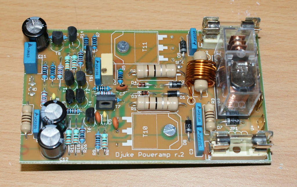
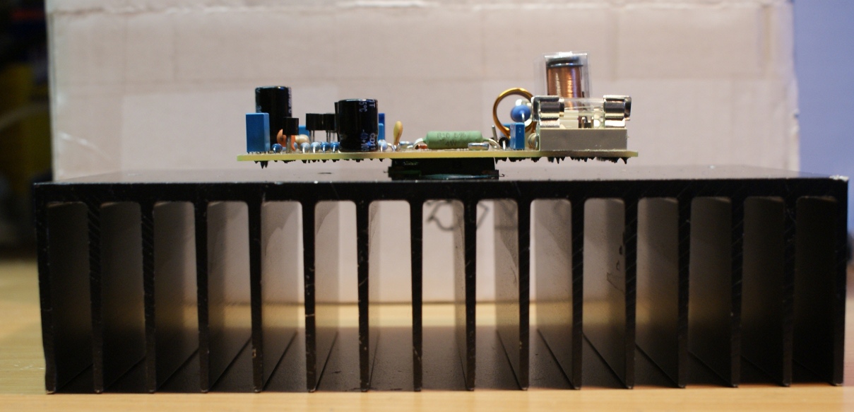
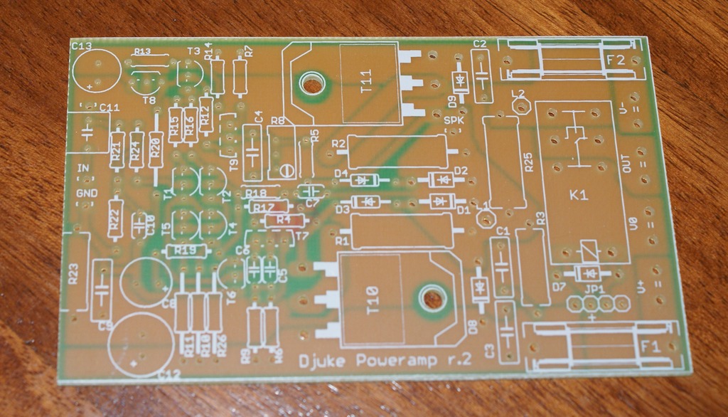
The amplifier pcb is a single-layer board, using only through-hole components. All the components, including fuses, output inductor and output relay are placed on a board of only 6x10cm in size! The MOSFET’s are located at the bottom of the board and the complete board can be attached to a heatsink using two bolts through the MOSFET’s. Photos of the empty and assembled pcb are shown next.
Mounting layout
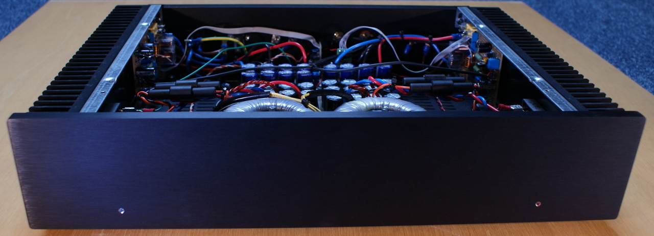
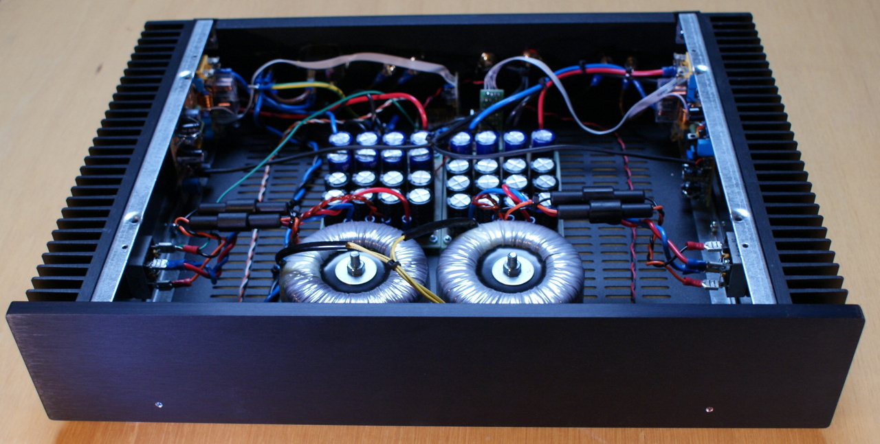
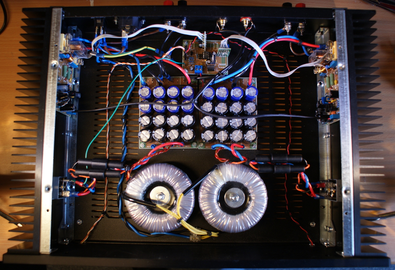
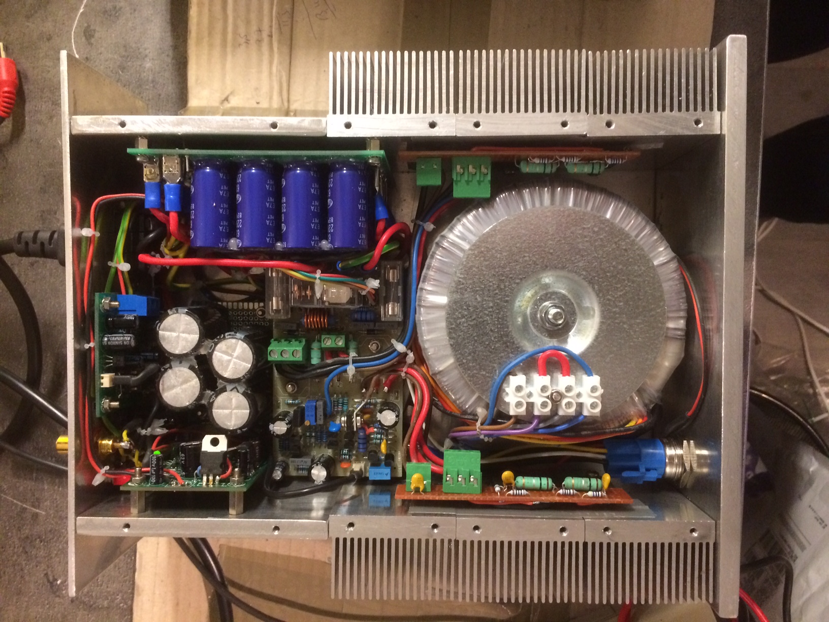
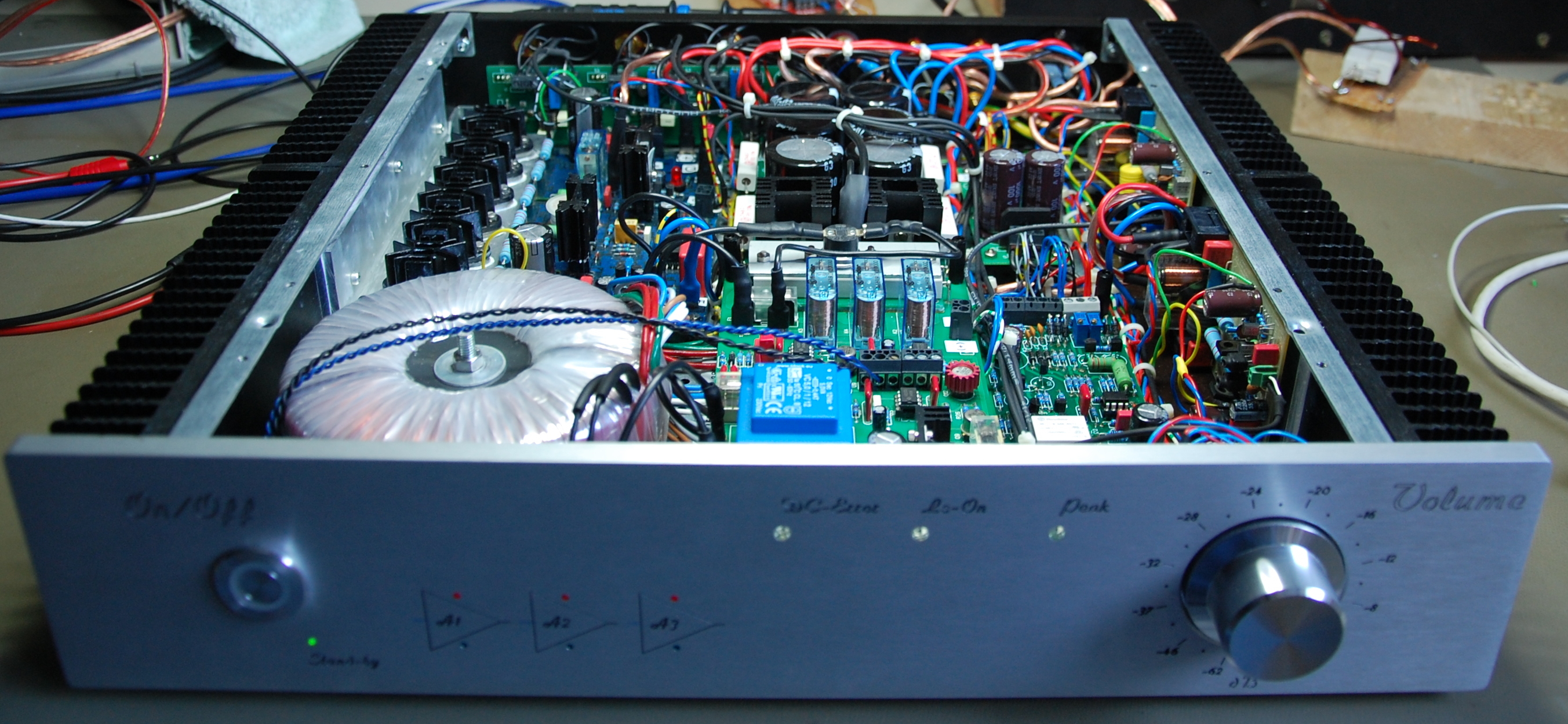
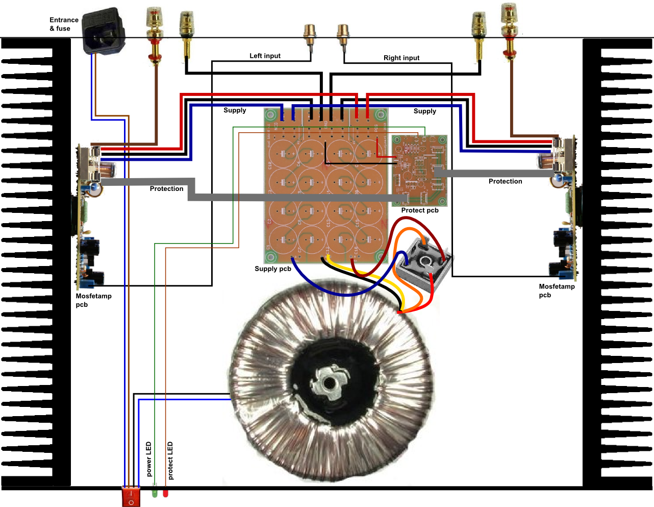
This mosfet power amplifier is very versatile, you can build several channels including filters or preamp in one cabinet. But maybe the most common use is a stereo power amplifier, for which the proposed mounting layout is shown in the next figure. To build it, the following components are needed:
- Cabinet (including heatsinks)
- Toroidal transformer
- 1x Power entry with fuse
- 1x Power switch
- 1x Bridge rectifier
- 1x Supply kit (pcb + components)
- 2x Mosfet amp kit (pcb + components)
- 1x PicProtection kit for 2 channels (main pcb, 2x detector pcb + components)
- Connectors (2x cinch, 2x speaker set)
- Various wiring
A complete stereo version of this power amp can be built for between EUR 300,- and EUR 350,-
Measurements
To measure the performance of my audio equipment I bought an E-mu 1212m sound card with outstanding performance. RMAA measurements of a loopback test with the card can be found here. To measure the performance of the amplifier, I used the following measurement setup:
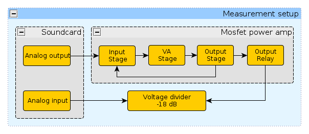
Because the output voltage of the mosfet amp is far too high to be connected directly to the analog input of the sound card, I used a simple voltage divider to attenuate this signal. This has some influence on the measurement results, especially the measured bandwidth, which seems lower, because the analog input of the sound card is not driven from a low impedance source anymore. THD and noise measurements are not influenced very much.
Test conditions:
- Measurements at 24-bit, 96kHz.
- Analog output set to about -3 dB before amp starts clipping
- Supply: 2x30V 225VA torroidal transformer, 35A bridge rectifier, 2x13200uF capacitor bank gives 42V dual supply
- Test performed with single (mono) amplifier board
- Test performed without output load
- Test performed with 8 ohm resistive load connected to amplifier output
Test results
| Test results | DjukePoweramp NoLoad | DjukePoweramp 8ohm |
|---|---|---|
| Frequency response (from 40 Hz to 15 kHz), dB: | +0.04, -0.23 | +0.04, -0.24 |
| Noise level, dB (A): | -102.5 | -102.3 |
| Dynamic range, dB (A): | 102.4 | 102.4 |
| THD (1kHz), %: | 0.0004 | 0.0007 |
| THD+Noise (1kHz) , % (A) | 0.0016 | 0.0021 |
| IMD + Noise, %: | 0.0022 | 0.0028 |
Most interesting graphs
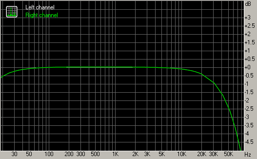
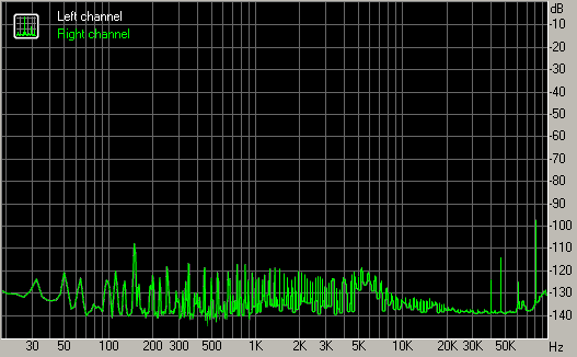
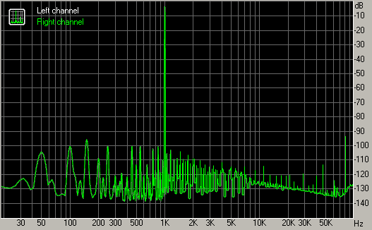
Frequency response, noise figure and total harmonic distortion measurements with 8 ohm load.
Measurement conclusions
- Frequency response seems to be measured at 55 kHz, but is actually about 100kHz. In the comparison graph, it can be seen that this is caused by limited bandwidth of the sound card and the voltage divider in combination with input capacitance of the sound card.
- Low side crossover frequency approximately at 7Hz, with 1uF input capacitor.
- Largest noise source -110dB @ 50Hz. May improve with somewhat larger capacitor bank
- THD without load is extremely low, which shows that the input stage and VA stage of the amplifier are quite optimal
- THD+N increases only slightly with 8ohm load (0.0016% -> 0.0021%)
- Largest THD contribution -108dB @ 2kHz, which is 2nd harmonic (even harmonics sound more pleasing than odd harmonics)
General conclusions
The designed amplifier not only measures well, but also sounds great. Describing the sound of an amplifier is always a very subjective thing, but anyway there we go: it sounds very transparent and is full of detail. The low regions are very clear and direct (I believe because of the absence of passive components in the speaker) and the mid is very detailed (due to the active LR-crossover) and high is very smooth (due to the amplifiers two pole compensation, distortion stays low also above 1kHz). I believe that further increase in performance of this amplifier, can only be achieved by using a symmetric mirror-image, which makes it bigger, more complex and most likely less reliable.
Gallery
